Mechanically Bistable MEMS Optical In-Plane Switch
KTH EK2360 — Hands-on Micro-Electromechanical Systems Engineering · Group 4, three students · Electrum Laboratory, Kista · November 2022 – January 2023
EK2360 is a course built around one uncomfortable fact: you design your device, you send it to a real cleanroom, and some weeks later you get back a wafer full of your own mistakes. There is one fabrication run and no second chance. Everything the group had assumed silently — about stiction, about symmetry, about whether a probe needle could actually reach a pad — arrives at once, under a microscope.
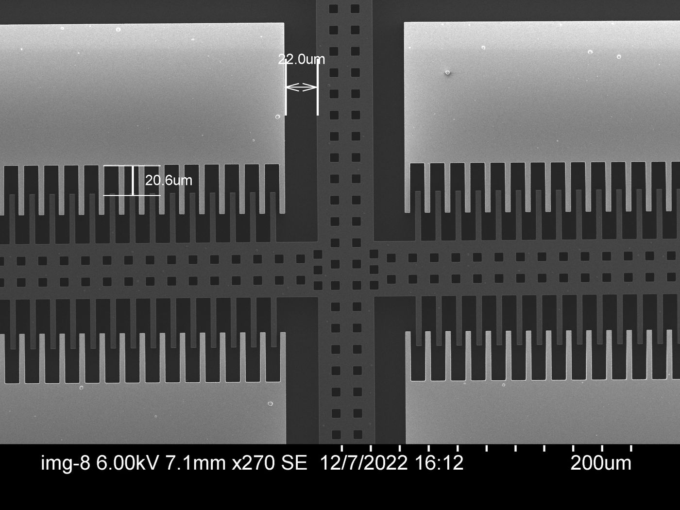 The device as fabricated, imaged in the SEM at 6 kV. The comb fingers, the etch holes in the moving
mass, and the released structure are all visible; the scale bar is 200 µm.
The brief
Design a mechanically bi/multi-stable optical in-plane switch for routing signals in a fibre network. A vertical micro-mirror sits at an X-crossing of two fibre paths and is pushed in or pulled out to send the light either straight through or around a 90° bend. The mechanical part of “bistable” is the point: the switch has to latch in both the full-in and full-out positions, so external power is needed only for the transition, never for holding state. Partially inserting the mirror turns the same device into a tunable attenuator.
The specification we had to hit:
| Requirement | Value |
|---|---|
| Total in-plane displacement | 30 µm between end positions |
| Passive restoring force at each end | 30 µN |
| Stiffness ratio, unwanted (y) vs wanted (x) | ≥ 50× |
| Analog positioning between the end points | required |
| Voltage sources | at most 2 |
| Maximum actuation voltage | 65 V |
| Largest actuator dimension | ≤ 1.8 mm |
| Process | SOI MEMS, 30 µm device layer |
Design
The actuator is an electrostatic comb drive: 40 fingers, 35 µm long and 4 µm wide, 3 µm gaps, with 12 µm of initial overlap. Comb drives are the right choice here precisely because their force is, to first order, independent of displacement — which is what gives the analog positioning the brief asked for.
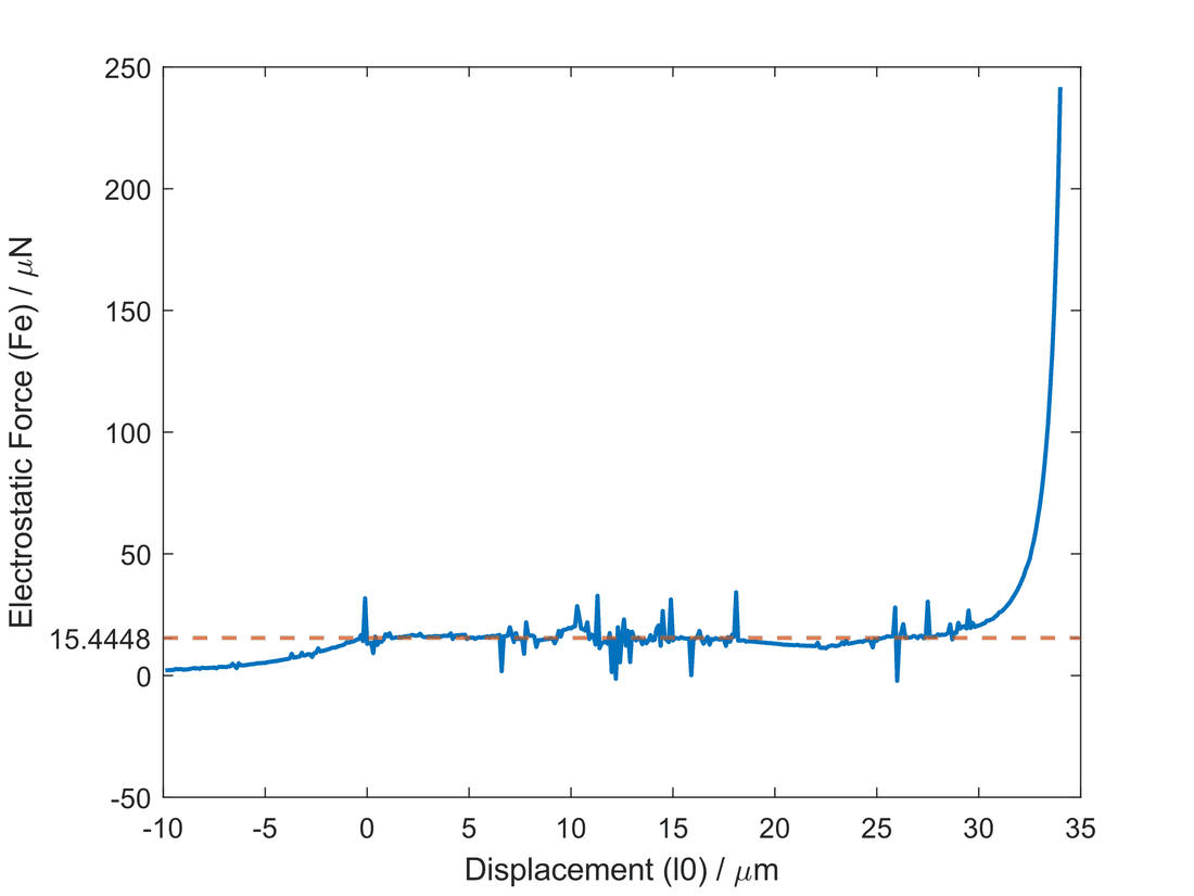 Simulated electrostatic force against displacement at 65 V. The plateau at 15.4 µN is the
constant-force range the design lives in; the wall at the right is pull-in, where the fingers snap
together and the device is over.
The restoring mechanism is a set of folded springs — 690 µm long, 4 µm wide, 30 µm thick — sized so that the spring force reaches the specified 30 µN at the end of travel. COMSOL put the stiffness at 2.146 N/m against a hand-calculated 1.987 N/m, an 8% gap that is about what you would expect between a beam formula and a meshed 3-D model.
 The folded-spring topology: compliant along the travel axis, stiff across it.
The hard part is the stiffness ratio. A comb drive pulls sideways as well as forwards, and if the lateral spring stiffness loses to the lateral electrostatic stiffness, the moving mass snaps into the fixed comb and welds itself there. We swept the lateral force against lateral displacement for three finger overlaps and checked it against the spring line:
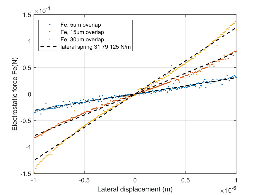 Lateral (side-instability) check. The dashed line is the lateral spring stiffness; the coloured
curves are the destabilising electrostatic force at 5, 15 and 30 µm finger overlap. Where a curve
climbs above the line, the design is unstable — which is why overlap is a design variable and not
just a number you pick.
The lock is a pair of parallel-plate actuators driving locking cantilevers: 302 µm plates at a 4 µm gap, producing 7.468 µN at 65 V, deflecting the cantilevers 3.28 µm — just enough to clear the latch. Calculated pull-in for that geometry is 23.2 V.
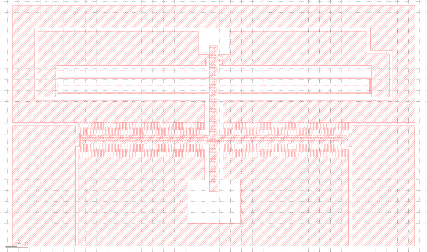 The final mask layout in KLayout: comb drives left and right of the central moving cross, folded
springs top and bottom, locking cantilevers and probe pads around the edge. Four design variants —
A1, A2, B1, B2 — went onto the chip so that the fabrication run would test more than one idea.
What came back
The chips were fabricated at Electrum and evaluated on a probe station.
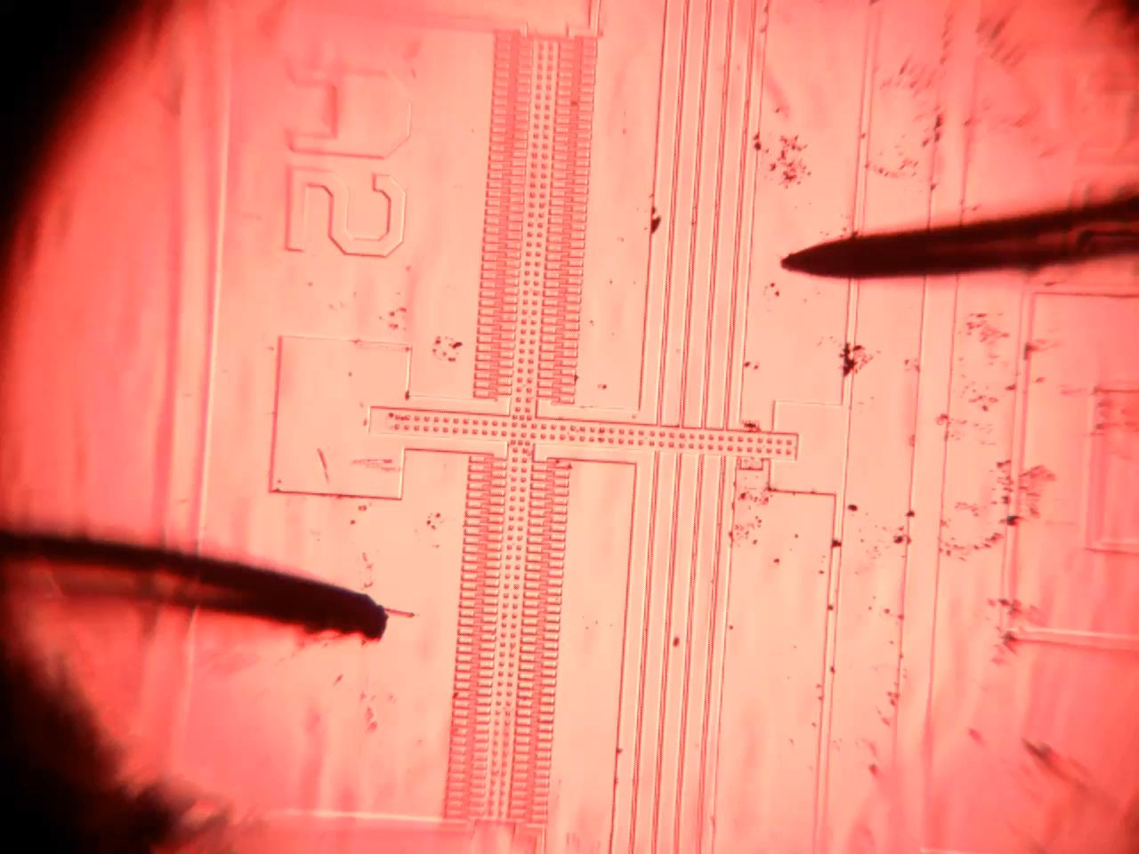 Two probe needles landed on the pads. The moving cross is in the centre; the comb fingers are the
fine hatching either side.
The device moves:
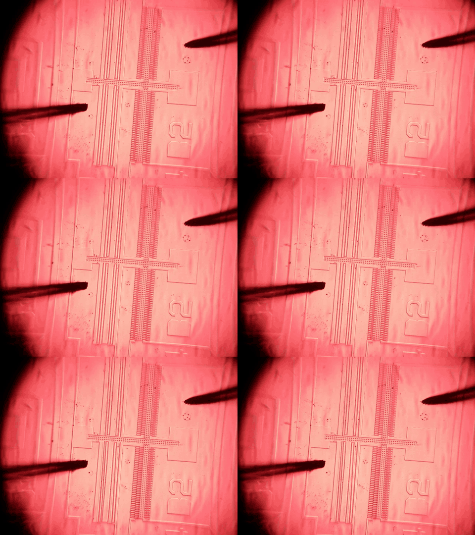 Design B actuating. Movement begins at around 26 V.
All four variants moved, at 26.3–26.6 V. None of them latched. And one of them did something we had not designed at all:
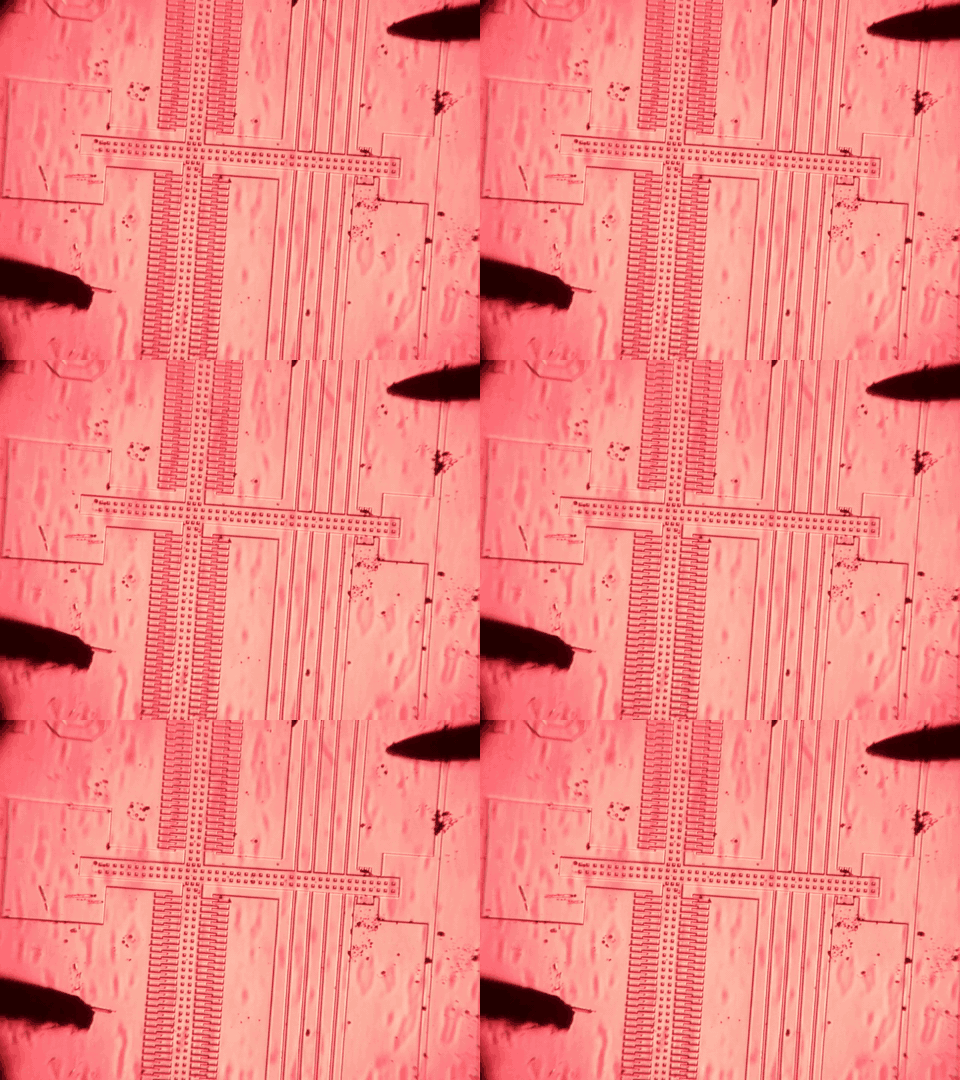 Design A2 during the oscillation test. The moving mass is rotating rather than translating — the
failure mode that turned out to explain most of the rest.
| Variant | Behaviour |
|---|---|
| A1 | Moves, but minimally. No oscillation. Locking mechanism faulty. |
| A2 | Stiction. Slight movement at 26.6 V. Poor rotational stability — rotates during oscillation. |
| B1 | Moves at 26.26 V. Lock cannot hold position once the voltage is removed. |
| B2 | Moves at 26.5 V. Stiction at the bottom on some chips. Obvious charging effect. |
Why it failed
This is the part worth writing down.
The rotational stiffness was under-specified, and we had the number. The brief recommended 10×10⁻⁹ to 100×10⁻⁹ Nm/degree. Our two spring arrangements simulated at 3.85×10⁻⁹ and 5.87×10⁻⁹ Nm/degree — both below the bottom of the recommended band. The paired three-spring layout was chosen because it lowers the resonant frequency, which it does; what it also does is give the moving mass a rotational degree of freedom that nothing is holding. The rotation visible in the GIF above is that number showing up in silicon.
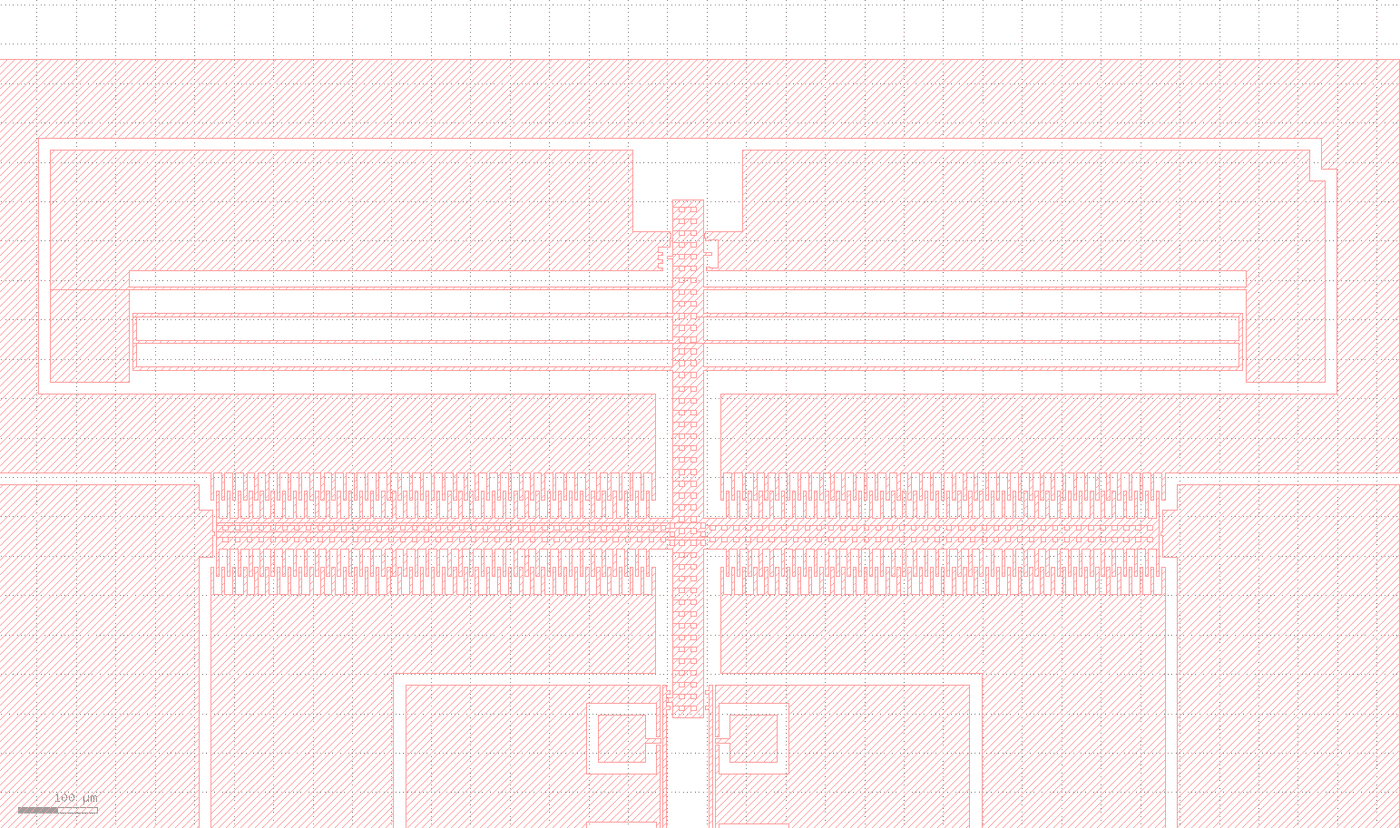
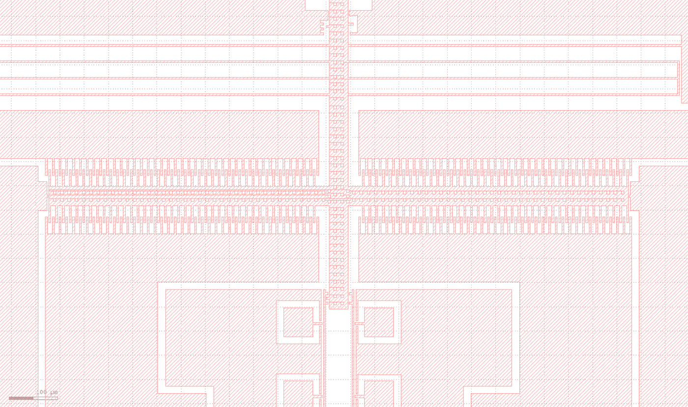 Comb flaw: the two sides do not carry the same number of fingers. An unequal finger count means an
unequal force, and an unequal force about the centre of mass is a torque — feeding directly into the
rotation problem above.
 Spring flaw: the paired three-spring arrangement trades rotational stability for a lower resonant
frequency. We knew about the trade; we did not weight it correctly.
The rest of the list:
- Stiction. Released structures at these dimensions stick — to the substrate, and in the lock, to each other. It is the classic MEMS failure and we did not design enough margin against it.
- The lock never held. Even where the cantilevers deflected, the latch could not retain the moving mass after the actuation voltage was removed. Without that, the whole premise of the device — bistability, zero holding power — is gone.
- Charging. Visible on design B2: dielectric charging shifts the effective actuation voltage as the device is driven, so the behaviour is not reproducible between runs.
- Layout ergonomics. Some pads were genuinely hard to land a probe on, and the poking area for mechanical testing was too small. These sound trivial until they cost you measurements on a chip you cannot re-fabricate.
- An unbalanced moving mass, which compounds every rotational problem above.
The calculated resonant frequency was 98.6 Hz.
The redesign
The final deliverable was a design revision for a next fabrication cycle that does not exist — which makes it a pure exercise in diagnosis.
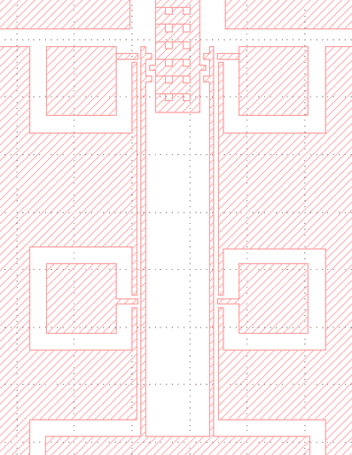 Lock: added the etch holes missing from the moving part, moved the stoppers closer to the
cantilevers’ edge, and added the right-hand lock that the original layout was missing outright.
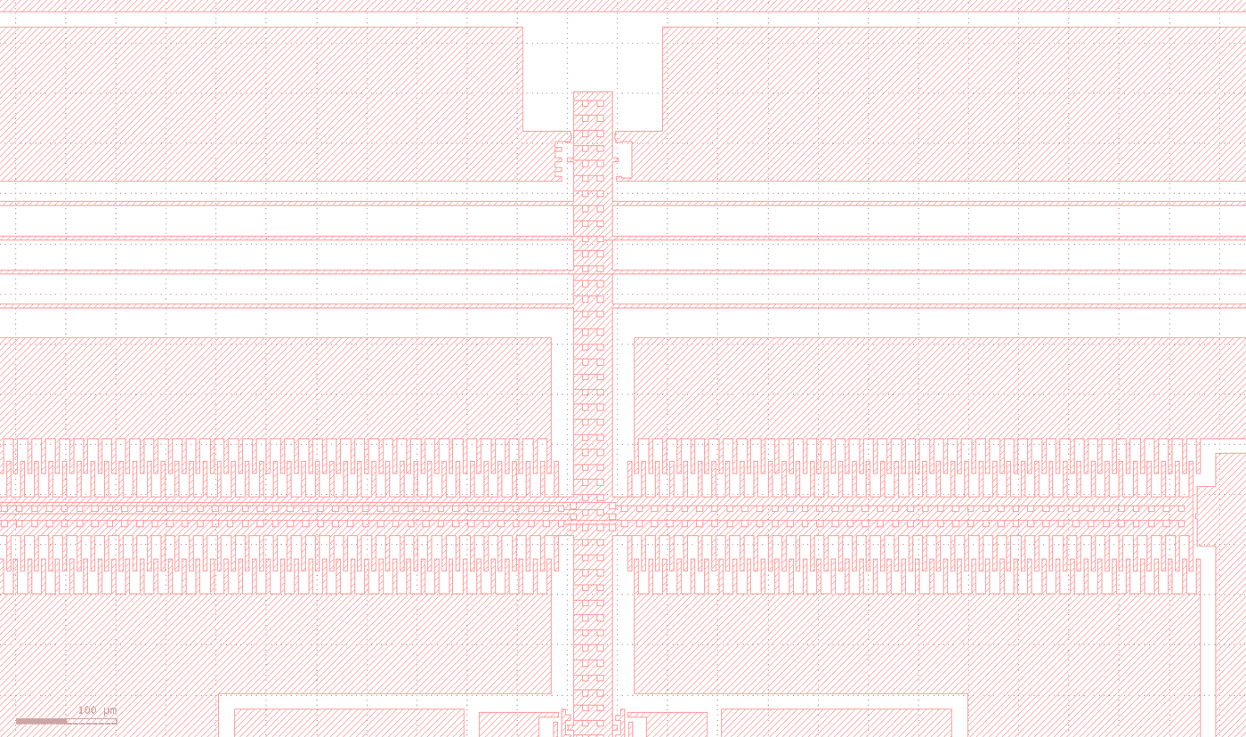 Comb and layout: one more finger to make the two sides symmetric, the tip moved to the balanced
position, read marks rearranged.
Plus: a re-designed spring aimed at the recommended rotational-stiffness band rather than the lowest resonant frequency, easier probe access, a larger poking area, and a properly balanced moving mass.
What I took from it
Three things, and none of them are about MEMS specifically.
The first is that we had the number that predicted the failure before we sent the design out. The rotational stiffness was simulated, written in a table, and below the recommended range — and we built it anyway, because it was one row among many and the design was otherwise finished. Simulating something is not the same as letting the result change your mind.
The second is that a one-shot fabrication run is an unusually honest teacher. There is no iterating your way out; the design you commit is the design you get, so the discipline has to happen before the run rather than after it.
The third is about the value of variants. The course splits each group into two sub-groups that develop competing concepts, so A1, A2, B1 and B2 all went onto the same chip — and they failed in different ways. Those differences are what made the diagnosis possible at all. A single design that did not work would have told us almost nothing about why.
Team
Group 4: Xuezhi Niu, Gianluca Zalla, Protik Pandey. Design, simulation, layout and evaluation were shared across all three of us throughout.
Course given by Joachim Oberhammer at KTH; fabrication in the Electrum Laboratory, Kista.